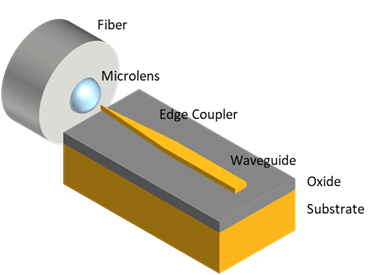
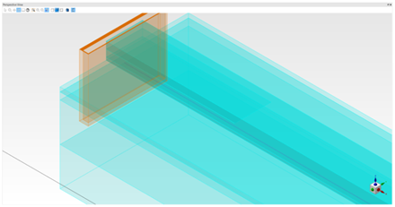
The microlens edge coupler is transforming fiber-to-chip integration, offering improved coupling efficiency, relaxed alignment tolerances, and streamlined photonic packaging. Efficiently coupling light from an optical fiber into a photonic chip remains one of the most critical challenges in photonics. The problem lies in bridging two very different optical domains: the relatively large mode field diameter of a single-mode fiber and the much smaller waveguide modes on a chip. This mismatch, combined with alignment sensitivity and packaging complexity, leads to significant insertion losses and increased manufacturing costs.
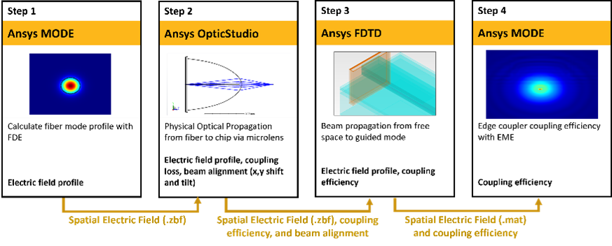
This workflow combines device-level and system-level simulations into one coherent process. By doing so, engineers can study each component in detail while also understanding its impact on the entire optical path.
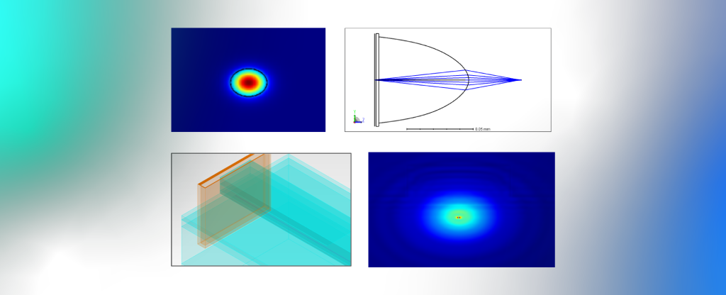
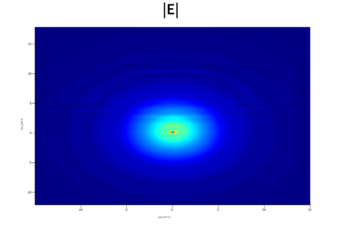
The fiber mode is then imported into OpticStudio and propagated through a microlens using Physical Optics Propagation (POP). This step is crucial because it evaluates the system’s tolerance to practical imperfections—such as lateral shifts, angular deviations, or defocusing.
The combined workflow offers several major advantages:
Investors increasingly consider ESG criteria, with over 80% of mainstream investors now factoring sustainability information into investment decisions. Companies implementing comprehensive sustainability strategies report up to 10% reduction in capital costs, making simulation’s environmental benefits financially material.
The Ansys Lumerical–OpticStudio workflow makes it possible to model this system from fiber to chip with high accuracy, bridging device-level nanophotonics and system-level optics in a single pipeline. For industries developing scalable silicon photonics, co-packaged optics, and quantum photonic platforms, this approach is not just a design tool—it’s a competitive advantage. By leveraging the microlens edge coupler, photonic designers can achieve efficient, scalable, and reliable fiber-to-chip connections for next-generation applications.