Efficiently coupling light from an optical fiber into a photonic chip remains one of the most critical challenges in photonics. The problem lies in bridging two very different optical domains: the relatively large mode field diameter of a single-mode fiber and the much smaller waveguide modes on a chip. This mismatch, combined with alignment sensitivity and packaging complexity, leads to significant insertion losses and increased manufacturing costs.
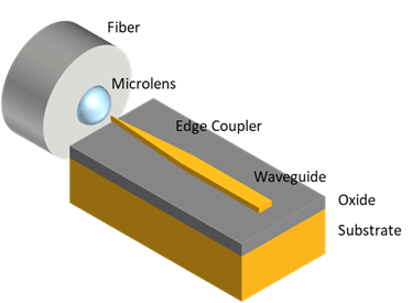
To address this challenge, engineers have been exploring various coupling schemes. Grating couplers offer wafer-level testing benefits but suffer from limited bandwidth and directionality. Edge couplers, on the other hand, can deliver high efficiency and broadband operation but require precise alignment. The integration of a microlens with an edge coupler introduces a clever compromise—expanding and reshaping the fiber mode before it reaches the chip interface. This approach relaxes alignment tolerances, improves coupling efficiency, and makes large-scale packaging more practical.
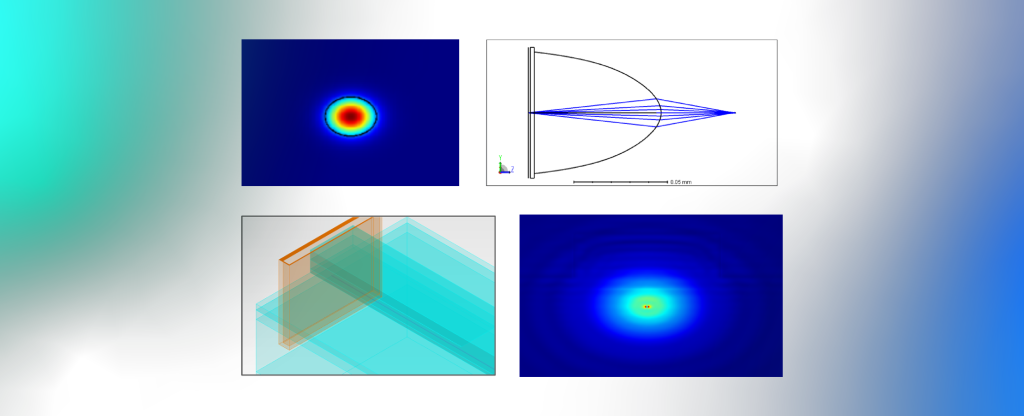
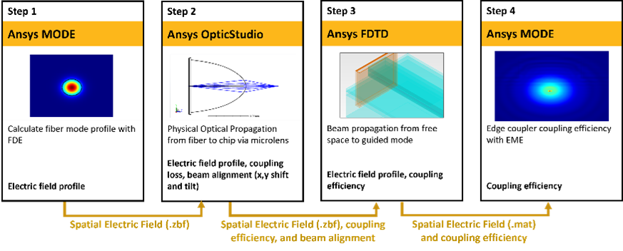
In this blog, we will explore a simulation-driven workflow using Ansys Lumerical (MODE, FDTD, EME) and Zemax OpticStudio (POP) to analyze and optimize a fiber-to-chip edge coupler with a microlens.
The journey begins with calculating the fiber mode. For example, in a standard SMF-28 fiber, the TE mode is solved using the Finite Difference Eigenmode (FDE) solver in Lumerical MODE. This mode field is then exported for further use.
This step ensures that the fiber’s optical characteristics are accurately captured before propagating into the microlens.
By expanding and collimating the beam, the microlens makes the coupling system significantly more forgiving to alignment errors.
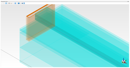
The reshaped beam is then imported into Lumerical’s Finite Difference Time Domain (FDTD) solver. Here, the free-space-to-chip interface is modeled in detail. Source offsets (lateral and vertical) can be applied to mimic misalignment scenarios, helping predict performance under real packaging conditions.
This stage captures detailed electromagnetic interactions at the chip surface, ensuring that diffraction, reflections, and mode overlap are all accurately considered.
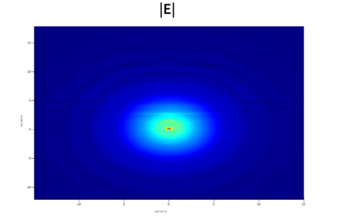
Finally, the optical field at the chip interface is fed into an Eigenmode Expansion (EME) simulation. This models the Spot-Size Converter (SSC) inside the photonic chip, which compresses the expanded mode into the much smaller waveguide mode.
At this stage, insertion loss contributions can be broken down into lens efficiency, interface loss, and SSC performance, providing a complete picture of system efficiency.
The integration of microlenses with edge couplers represents a powerful advancement in fiber-to-chip coupling. By combining the beam-shaping advantages of microlenses with the efficiency of edge coupling, this method significantly reduces insertion loss while increasing packaging tolerance.

