Every new product promises to be smarter, smaller, faster, and more efficient. But behind that sleek exterior is a complex engineering puzzle that continues to get harder every year.
Modern devices are no longer simple electronic assemblies. They are complex integration of magnets, coils, power electronics, sensors, controllers, processors, and wireless communication elements, all filled into tight packages that continue to shrink. With this complexity comes unexpected challenges like electromagnetic interference, heat buildup, structural stress and system-level interactions that are nearly impossible to predict through traditional testing of a prototype alone.
This is exactly why more companies are turning towards engineering simulation, especially low-frequency electromagnetic simulation as the backbone of their design process.
A decade ago, wiring up a new electronic product and testing it on the bench was enough to validate a design.
Today, even a simple conductor inside a compact gadget can behave like an antenna, radiating unwanted electromagnetic noise. High-speed processors interact with power modules. Sensors sit next to inductors. Wireless coils operate close to temperature-sensitive components. A vent that improves heat flow might allow higher EMI leakage.
Everything is interconnected…!!
A tiny mistake, even a minor change in material properties, coil spacing or PCB layout can create problems that show up only after a product reaches the customer. Simulation has become essential because it reduces these unknowns before they become expensive mistakes!!
Rather than waiting until the prototype stage to discover issues, engineers now can simulate the entire device early in the design cycle. This lets them visualize exactly how electromagnetic fields behave, how heat flows inside the device, how structural parts deform, and how different subsystems influence one another. Some of the biggest advantages include:
Engineers can try hundreds of “what-if” scenarios like coil shapes, magnet materials, PCB layouts, vent sizes, motor geometries without building a single prototype.
Testing only tells you whether a design passes or fails.
Simulation tells you why it behaves the way it does.
Many interference problems, losses, and coupled-physics effects only appear in the virtual prototype tests.
Ansys Maxwell: The engine for electromagnetic accuracy
Maxwell is widely used to design:
It gives engineers a deep view of magnetic field behaviour, losses, torque generation, inductance, saturation, and force, all before a physical prototype exists. For compact consumer devices, this accuracy is crucial.
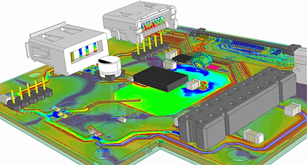
Fig.1 Electromagnetic Field Visualization in a PCB Assembly
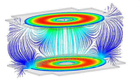
Fig.2 Magnetic Field Distribution in a Wireless Power Transfer System
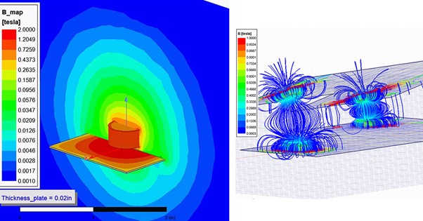
Fig3. Ansys Maxwell Simulation of Magnetic Latching Fields
In many consumer products, solving one problem creates another. Multiphysics simulation reveals these hidden interactions so engineers can make the right trade-offs.
Every year, customers expect more performance, features, intelligence, efficiency in a smaller device. This level of innovation is impossible through trial-and-error design. It demands a deeper understanding of physics, the one that only simulation can provide.
With the simulation tools under Ansys ecosystem, engineers can explore ideas freely, refine them faster, and ensure their products are reliable before they ever reach the market.
Simulation isn’t merely just a tool for validating ideas; it is becoming the starting point for creating them…!!