Edge couplers are vital components in photonic integrated circuits (PICs), facilitating efficient light transfer between optical fibers and on-chip waveguides. The Ansys Optics article provides a comprehensive guide on designing and optimizing edge couplers, particularly for silicon-on-insulator (SOI) platforms operating at a 1550 nm wavelength.
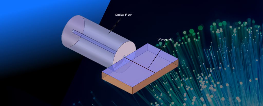
Edge couplers function by aligning an optical fiber directly to the edge of a photonic chip, allowing in-plane light coupling. This method is especially beneficial for applications requiring high coupling efficiency and broad bandwidth.
The design process utilizes simulation tools like the Eigenmode Expansion (EME) method to optimize parameters such as fiber position and taper length, achieving a modal overlap efficiency of approximately 93%.
Edge coupler 3D view
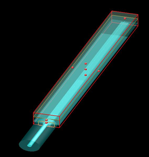
Designing an edge coupler involves a series of simulation and optimization steps to ensure efficient light transfer between a single-mode fiber and an on-chip waveguide. Here’s a concise overview of the procedure based on the Ansys Optics workflow
This structured simulation flow ensures optimal coupling efficiency, minimal loss, and compatibility with fiber interfacing in PIC applications.
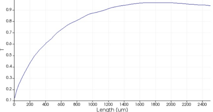
EME sweep data of taper length
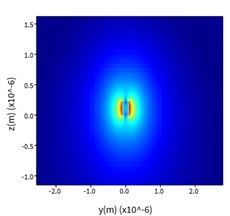
Output mode
In PICs, several coupling techniques are employed, each with its advantages and limitations:
Grating couplers use diffractive structures to couple light vertically into the chip.
|
Advantages
|
Limitations
|
|---|---|
|
Flexible Placement – Can be positioned anywhere on the chip surface.
|
Lower Coupling Efficiency –Typically below 3 dB.
|
|
Wafer-Level Testing – Facilitates testing before chip dicing.
|
Narrow Bandwidth – Limited operational wavelength range.
|
|
Compact Size – Occupies minimal chip area.
|
Polarization Sensitivity – Performance can vary with light polarization.
|
Evanescent couplers rely on the overlap of evanescent fields between adjacent waveguides.
|
Advantages
|
Limitations
|
|---|---|
|
High Coupling Efficiency – Often around 1.0 dB.
|
Complex Fabrication – Requires precise control over waveguide spacing.
|
|
Broad Bandwidth – Suitable for wavelength-division multiplexing.
|
Limited to Specific Designs – Not as versatile for all PIC layouts
|
|
Good Alignment Tolerance – Less sensitive to positioning errors.
|
As discussed, edge couplers offer high efficiency and broad bandwidth but come with their own set of challenges.
|
Advantages
|
Limitations
|
|---|---|
|
High Coupling Efficiency – Approximately 1.2 dB insertion loss.
|
Fabrication Complexity – Requires precise cleaving and polishing of the chip edge.
|
|
Wide Bandwidth – Up to 200 nm for TE modes.
|
Fixed Coupling Position – Limited to the chip's edge, restricting design flexibility.
|
|
Polarization Independence – Less sensitive to light polarization.
|
Larger Footprint – Occupies more space compared to grating couplers.
|
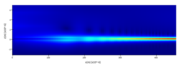
Mode profile in x-z plane
Edge couplers are indispensable for applications demanding high coupling efficiency and broad operational bandwidth in photonic integrated circuits. While they pose fabrication and design challenges, their performance benefits often outweigh these drawbacks, especially in high-speed data communication systems. When selecting a coupling method, engineers must balance factors like efficiency, bandwidth, fabrication complexity, and design flexibility to meet specific application requirements.